- 中文简体
- 中文繁体
- English
- Русский
- 日本語
- 한국 사람
- Français
- Deutsch
- हिंदी
- Português
- Español
- بالعربية
- Corsu
- guarani
- kinyarwanda
- Hausa
- Norge
- Nederlands
- Yoruba
- गोंगेन हें नांव
- Latina
- नेपालीName
- čeština
- ʻŌlelo Hawaiʻi
- ჯორჯიანიName
- فارسی
- भोजपुरी
- беларускі
- Kiswahili
- ÍslandName
- ייַדיש
- tur
- Gaeilge
- ગુજરાતી
- Slovenská
- היברית
- ಕನ್ನಡ್Name
- Magyar
- தாமில்
- بالعربية
- বাংলা
- Azərbaycan
- lifiava
- IndonesiaName
- dansk
- Shona
- Bamanankan
- Lietuva
- Tiếng Việt
- Malti
- Türkmençe
- অসমীয়া
- català
- සිංගාපුර්
- Suomalainen
- Кыргыз тили
- Eʋegbe
- Hrvatski
- a n:n
- Quechua
- bosanski
- Maori
A well-known problem in GaN HEMTs is dynamic  (
( ), where
  is larger than its measured dc value following severe blocking voltage stress.
  does not frequently appear in datasheets, although it causes unfavorable increases in the device's conduction loss and junction temperature.
Especially for high-frequency applications, this  , presents significant design issues for GaN-based power converters. Various factors affecting the
  are its physical characteristics, factors affecting the number of trapped electrons, and the characterization approach.
Physical Characteristics
The trapping effect can cause  to develop in a number of different parts of the GaN HEMT's structure. Charge trapping could happen in the buffer layer, the GaN channel, the gate region, close to the surface, and/or in the dielectric due to the following reasons:
● Leakage current electrons being inserted under high drain bias
● Hot electrons are created during switching transitions, which are the result of the overlapping of high voltage and high current
All of them have the potential to lessen 2DEG conductivity while simultaneously raising  . At the device level, a number of methods have been put forth to lessen trapping effects and solve the
  problem, including
● Surface passivation optimization
● Intricately constructed GaN buffers
● Ideal field-plate structures
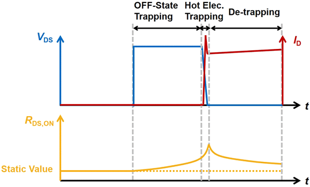
The typical  variation of GaN HEMTs during a switching event is seen in Fig. 1.
  increases primarily in two stages:
● Hard turn-ON
● OFF-state

Fig. 1.  variation during a switching event of GaN HEMTs. Source: IEEE Transactions on Power Electronics
Hard Turn-ON
The hard turn-ON process has a more significant impact on the  than the OFF-state process. The hard turn-ON stress causes electron trapping both in the buffer and at the interface that lies between AlGaN and the passivation layer.
According to several studies, interface/surface trapping predominate during the hard turn-on process while observing the effect buffer region and the drain field plate. The energy level of the traps crucial to the hard turn-on process is widely dispersed but relatively shallow.
OFF-State
The OFF-state stress primarily causes electron trapping in the buffer. Detrapping these electrons in the on-state enables them  to gradually return to their static values. In most GaN HEMTs, it should be noted that the soft turn-ON procedure is not anticipated to cause considerable
  .
.
- Prev:None
- Next:Getting Started with Raspberry Pi: A Beginner's Guide
Recommend News
-
Tel
+86-0755-83269835 -
E-mail
-
Whatsapp


